Executive Summary
AI chiplets combined with 3D and heterogeneous integration represent the defining architectural shift for next- generation artificial intelligence hardware. Traditional monolithic System-on-Chip (SoC) and ASIC process shrinks are no longer commercially viable due to soaring development costs, complex manufacturing yields, and physical reticle size limits. While AI and machine learning workloads demand massive compute capacity—expected to grow 10x over the next 3–4 years—traditional I/O bandwidth only doubles every eight years. To bridge this critical bottleneck, the industry is pivoting toward "More than Moore" methodologies, positioning advanced package design at the absolute center of the electronics universe.
1. Introduction
AI and machine learning workloads demand a 10x compute increase over the next 3–4 years, yet traditional I/O bandwidth only doubles every eight years. Compounding this bottleneck, monolithic ASIC scaling has hit a wall due to skyrocketing costs, physical reticle limits, and soaring power consumption.
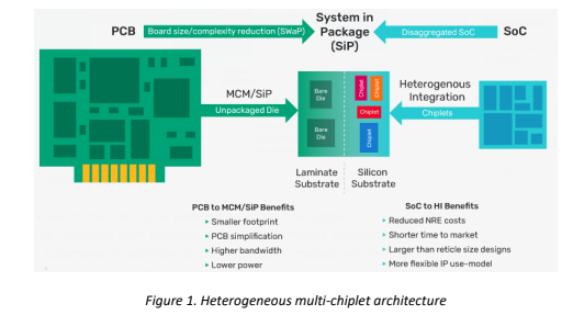
To break through, the industry is pivoting to heterogeneous 3D integration and modular chiplets (Figure 1). By partitioning functions like AI acceleration and I/O into separate dies, designers can optimize compute independently and upgrade systems without risky, full-chip redesigns.
However, chiplet effectiveness depends entirely on high-speed interconnects. Managing this complexity requires a shift to unified system-level design. Designers need a novel platform that aggregates data across IC, package, and board domains to optimize system-level Power, Performance, and Area (PPA) and ensure flawless signoff connectivity verification.
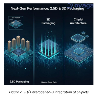
3D Heterogeneous Integration (3DHI) is an advanced design and manufacturing approach that integrates multiple semiconductor components, often built using different process technologies, into a single vertically stacked system. Unlike traditional planar designs, 3DHI enables tighter interconnects, shorter signal paths, and greater functional density.
Technologies such as 2.5D packaging, 3D stacking, TSV (Through-Silicon Vias), and chiplet-based architectures are redefining how chips are designed, connected, and optimized. These packaging paradigms enable massive bandwidth increases, lower latency, improved power efficiency, and greater functional integration—all without relying solely on smaller process nodes.
2. Problem Statement
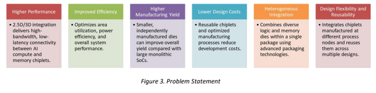
As monolithic System-on-Chips (SoCs) face severe physical limitations in scaling performance, yield, and cost, chiplet-based heterogeneous integration offers a powerful alternative. By utilizing advanced 2.5D and 3D packaging technologies, this architecture integrates diverse functional dies into a highly optimized, high- performance chip system. It allows designers to mix, match, and reuse dies fabricated across different process nodes for multiple projects. Consequently, this approach significantly overcomes traditional layout barriers, increases total chip yields, reduces time-to-market, and optimizes power, performance, and overall design costs.
3. Evolution of advanced multi-chiplet packaging technologies
4. Architectural Attributes of AI Chiplets and 3D/Heterogeneous Integration
A 3D integrated circuit (3D-IC) fuses vertical stacking and chiplet integration to assemble complete computing systems in tight physical proximity. By partitioning large systems into smaller functional chiplets and aligning them vertically via fine-pitch interconnects, this architecture achieves high performance, design flexibility, and efficient system scaling without relying solely on transistor miniaturization.
Vertical Stacking & Interconnects: Minimizes communication paths to slash latency, boost bandwidth, and lower energy consumption—crucial for data-intensive workloads
Heterogeneous Mixed-Node Integration: Pairs advanced compute logic tiles with mature, power-efficient I/O and analog technologies from different process nodes or foundries to optimize manufacturing costs.
Enhanced Memory Locality: Stacks high-bandwidth memory (HBM) directly atop or beneath GPUs and AI accelerators, providing massive vertical data channels that eliminate off-chip data-movement overhead.
Together, chiplets and vertical stacking form the foundation of today's scalable, high-yield multi-die systems.
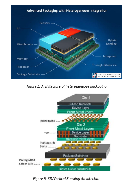
5. Heterogeneous Packaging Technologies
Advanced semiconductor packaging uses high-density interconnects, specialized routing, and optimized electrical and thermal designs to connect devices to the package and one another. It integrates single or multiple dies, chiplets, memory stacks, and passive components. To protect manufacturing yields, each component is fully tested before assembly; only those verified as known-good dies (KGDs) are selected, minimizing the risk of including defective parts in costly multi-die packages.
The dies are then arranged according to the package design:
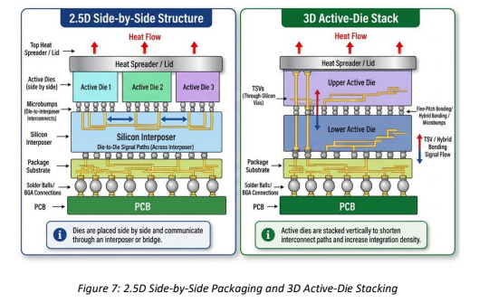
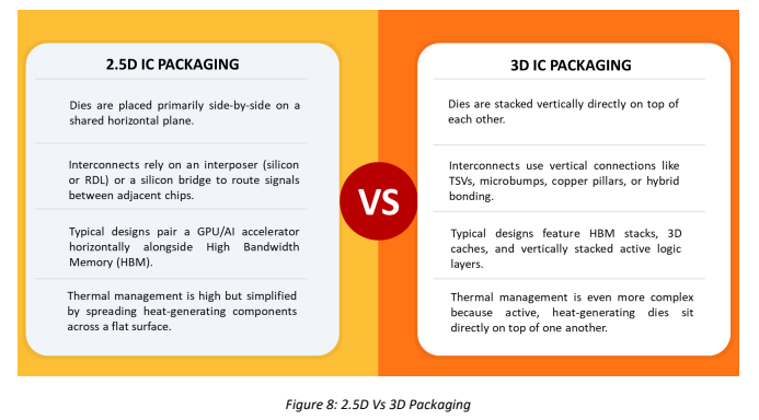
2.5D Packaging: Active dies are placed side by side and connected through a high-density interposer, bridge, or redistribution layer (RDL).
3D Packaging: Active dies are stacked vertically and connected using technologies such as microbumps, hybrid bonding, and through-silicon vias (TSVs).
6. 2.5D Vs 3D Packaging Techniques
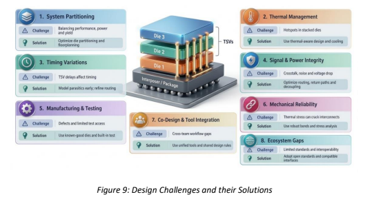
7. Design Challenges and Solutions
3D-IC technology delivers remarkable advancements in form factor, performance, and power efficiency. However, it also presents significant design challenges requiring innovative solutions across multiple domains. Below is an overview of these challenges and corresponding strategies:
8. IP Activity in AI Chiplets and 3D/Heterogeneous Integration
As part of our analysis of AI chiplets and 3D/heterogeneous integration technologies, an IP landscape study was conducted to identify patent applications related to advance semiconductor packaging, disaggregated chip architectures, vertical stacking methodologies, high-density interconnects, and associated thermal management techniques. A total of 4,778 patent applications (EFAM) were identified and analyzed.
8.1 Relevant keywords, synonyms and classes used for search
- 3D integrated circuit (3D-IC), Vertical die stacking, Stacked-die integration, TSV-based 3D integration, Vertical multi-die packaging
- Chiplet, Die, Modular semiconductor die, Dielet, Functional die, Disaggregated die, Chiplet-based building block
- Multi-chiplet architecture, Disaggregated SoC architecture, Modular IC architecture, Heterogeneous computing architecture, Chiplet-based system architecture
- 3D-IC thermal management, Chiplet cooling, Thermal-aware chiplet design, Package-level heat dissipation, Die-stack thermal control
- D2D interconnect, Die-to-die interface, Inter-die communication link, Chiplet-to-chiplet link, Die-to-die physical interface (D2D PHY)
- Relevant patent classification includes H10W90/297, H10W90/20, H10W70/611, H10W40/00, H10W70/635
8.2 Graphical Analysis from the identified patents (4778):
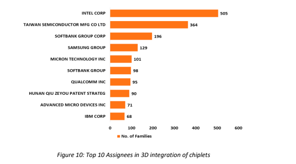
Figure 10 represents the key companies and their patent portfolios related to 3D or heterogeneous integration of chiplets, providing insights into the competitive landscape and innovation trends in this domain.
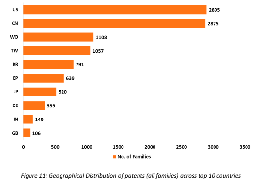
Figure 11 shows the distribution of patents across countries (top 10), providing insight into major R&D locations for working AI Chiplets and 3D/Heterogeneous Integration. USA has most patents followed by China. India also holds 9 th position.
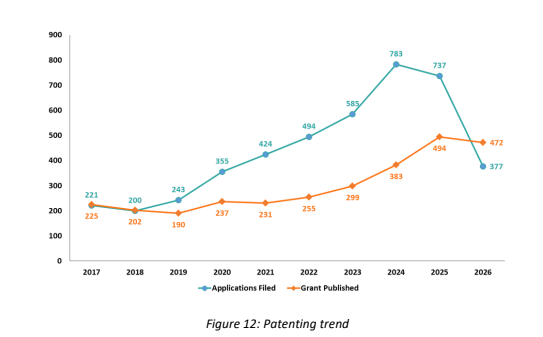
Figure 12 shows the patenting trend over the last decade (2017–2026). The patenting trend shows an overall increase in patent application filings from 2017 to 2024, rising from 221 to a peak of 783 applications. Although filings declined slightly in 2025 to 737, the data still indicates strong patenting activity. The number of published grants also generally increased, from 225 in 2017 to 494 in 2025, reflecting growth in patent grants over the period. Also, in 2026, applications filed decreased to 377, while grant publications reached 472.
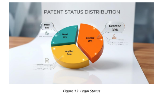
Figure 13 shows a pie chart demonstrating the total number of active (i.e., granted and applied) and inactive (i.e., dead) patents.
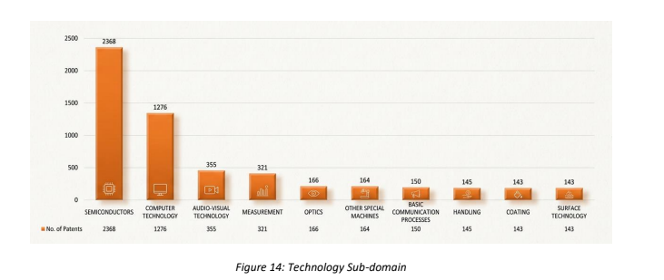
Figure 14 shows the technology-subdomain distribution for most patents or technology-record activity is concentrated in Semiconductors and Computer Technology with 2368 patents followed by the Computer Technology subdomain.
9. Market and Commercial Outlook
9.1 Global Chiplet Packaging for AI & HPC Market Outlook (2026-2035)
The global Chiplet Packaging for AI & HPC Market is projected to grow from USD 20.10 Billion in 2025 to USD 90.92 Billion by 2035, registering a 16.30% CAGR. Driven by AI and HPC demand for tightly coupled processors and memory, chiplet packaging circumvents the cost and yield limits of large monolithic chips by combining specialized dies using advanced 2.5D, 3D, and fan-out technologies. While adoption is accelerated by open standards like UCIe, massive customer orders, and public incentives—highlighted by Intel's December 2025 preview of a multi-chiplet design 12 times larger than current AI chips—the market faces constraints from thermal management, substrate supply, and packaging capacity.
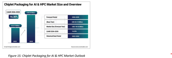
Source: https://www.snsinsider.com/reports/chiplet-packaging-for-ai-and-hpc-market-11228
9.2 Regional Chiplet Packaging for AI & HPC Market Outlook (2026-2035)
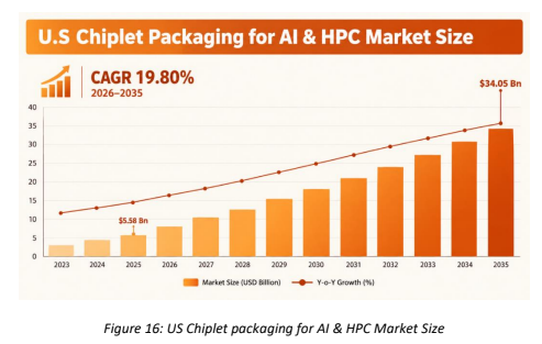
"Source: https://www.snsinsider.com/reports/chiplet-packaging-for-ai-and-hpc-market-11228"
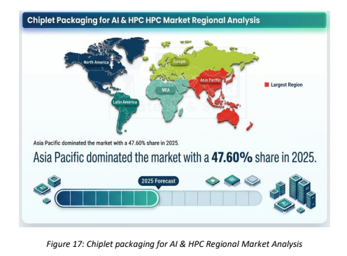
The global chiplet packaging market reflects distinct regional dynamics, led by Asia Pacific’s dominant 47.60% market share in 2025, which remains the industry hub driven by Taiwan's advanced foundries, China's self- sufficiency push, South Korea's memory, and Japan's materials. Meanwhile, North America clocks the fastest growth at a 19.80% CAGR (2026–2035), propelled by premier US chip designers using public and private capital to build domestic capacity in states like Arizona, with Canada and Mexico supporting. Europe maintains a strategic technology footprint via the European Chips Act, anchored by Germany's automotive demand, The Netherlands' lithography systems, and France/Belgium's advanced research, though its commercial manufacturing scale still lags behind.
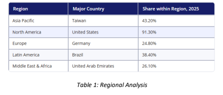
"Source: https://www.snsinsider.com/reports/chiplet-packaging-for-ai-and-hpc-market-11228"
"Source: https://www.snsinsider.com/reports/chiplet-packaging-for-ai-and-hpc-market-11228"
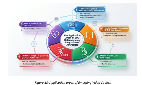
10. Applications Area of AI Chiplets and 3D/Heterogeneous Integration
11. Conclusion
The transition to 3D/heterogeneous integration marks a shift from monolithic silicon dies toward manufacturing complete computing systems as a single, integrated package. Utilizing advanced technologies like CoWoS, SoIC, Foveros, EMIB, hybrid bonding, and UCIe, this architecture combines specialized dies and memory to satisfy the data-movement demands of AI and HPC. However, scaling this market requires solving critical physical constraints in thermal management, power delivery, testability, yields, and cost. Future progress hinges on coordinated co-design across architecture, materials, interconnects, and cooling to create reliable, cost-effective systems that fully justify the complexity of heterogeneous integration.
How Pitch Scientific supports in AI Chiplets and 3D/Heterogeneous Integration
Pitch Scientific combines advanced semiconductor domain expertise with IP intelligence to help clients navigate emerging chiplet architectures and advanced packaging technologies, including 2.5D/3D integration, hybrid bonding, CoWoS, EMIB, and open interconnect standards like UCIe.
We support clients across the technology lifecycle through:
1. Prior Art & Patentability Searches:Identify relevant patents and prior art to assess the novelty and
patentability of new chiplet designs, advanced interconnects, and packaging methods.
2. Freedom-to-Operate (FTO) Analysis:Evaluate potential patent risks associated with developing and
commercializing multi-die architectures and heterogeneous systems.
3. Patent Landscape & Competitor Analysis:Map global patent portfolios, key players, and technology trends
across advanced packaging and die-to-die interface technologies.
4. White-Space Analysis:Identify technology gaps and engineering opportunities to guide future R&D in
heterogeneous integration and patent filing strategies.
5. Commercialization & Licensing Support:Help clients assess, position, and commercialize chiplet-related IP
portfolios, including identifying strategic licensing and partnership opportunities.
6. Ongoing Patent Monitoring:Track new patent filings, grants, packaging standards developments, and
competitor activity in the AI and HPC chiplet ecosystem.
By combining deep semiconductor expertise with strategic IP intelligence, Pitch Scientific helps clients reduce IP risks, strengthen patent portfolios, identify licensing opportunities, and accelerate the development and commercialization of next-generation heterogeneous computing technologies.


